How to use JTAG on MPC824x (sandpoint) boards
In the following example I will show how to use the JTAG port of an
MPC824x based NAS board without expensive, specialized hardware and software.
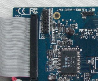
The target board is an Allnet 6250 NAS (a Netronix NH-230 clone), which had
been "turned into a brick" (it is dead), because the bootloader in the flash
chip was overwritten.
The process of resurrecting such a device by writing a new bootloader into
the flash via a JTAG cable is often refered to as "unbricking" or
"debricking".
Hardware used is a
ByteBlasterMV
cable, which is cheap to buy or to build yourself. Schematics are included
in the linked PDF document. You will, however, have to replace the 10-pin
Altera connector with a 16-pin PowerPC JTAG/COP connector. This is a cable
for the parallel port. Solutions for the USB port do exist as well,
but are not discussed here.
Software used is UrJTAG, which is
open source, runs on all BSD, Linux or Windows operating systems and gives
us the possibility to fix it ourselves, when there are problems. It is
the successor of openwince and one of the few programs which support
the MPC824x.
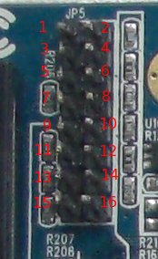
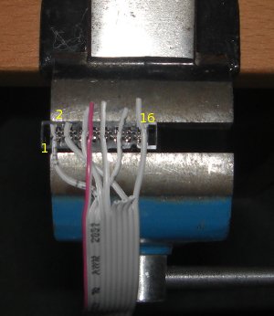
Soldering the JTAG interface header
|
Most boards come without a JTAG header soldered. Look for two
rows of eight holes each on the board, as in the picture to the right.
Often the holes are filled with solder, which must be removed
first. Do this either with a desoldering pump or some other technique
(like blowing the solder out of the holes).
You will probably solder two strips of 8 pins each forming the PowerPC
JTAG/COP header. When finished, it will look like the picture at the
left.
|
|
|
The pinout of the header is shown on the right.
Although the COP header defines more signals, we will only use
the four JTAG signals: TDO, TDI, TCK and
TMS. /TRST, to reset the JTAG logic, is not actually
required. The unused pins can be left unconnected in our cable.
It is guaranteed that the board has pull-up resistors installed
to keep signals like /QACK or /TRST high.
Of the JTAG signals only TDO is an output on the target
board; the other lines are input. This means our cable will drive
those input lines and receive something via TDO.
|
| Pin | Function | Pin | Function |
|---|
| 1 | TDO | 2 | /QACK |
| 3 | TDI | 4 | /TRST |
| 5 | HALTED | 6 | VREF |
| 7 | TCK | 8 | n.c. |
| 9 | TMS | 10 | n.c. |
| 11 | /SRST | 12 | GND |
| 13 | /HRST | 14 | n.c. |
| 15 | CKSTP | 16 | GND |
|
|
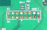
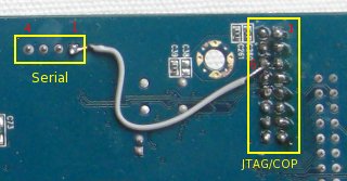
Power for the JTAG cable
|
The Byteblaster JTAG cable, and probably others too, is designed
to be supplied with power from the target board. For the
ByteblasterMV this is 3.3V. Unfortunately the PowerPC JTAG/COP interface
has not defined any pin to be used as a power supply. There is just
VREF, which indicates that the target has power. This signal is
usually connected via a 1K resistor to the board's 3.3V power supply.
But it is not enough to drive the circuits on a JTAG cable. The power
will drop to 1.7V (I tried it).
The solution is to establish a stable power supply from somewhere
else, for example from the VCC pin of the serial port.
On the All6250 the four pins of the serial header are near the JTAG
interface. Pin 1 is VCC (3.3V), which we can connect with
a wire to pin 6 of the JTAG interface (VREF), as shown in
the picture. Now there is sufficient power for the cable.
|
|
Building the JTAG connector
| Pin | Function | Pin | Function |
|---|
| 1 | TCK | 2 | GND |
| 3 | TDO | 4 | VCC |
| 5 | TMS | 6 | n.c. |
| 7 | n.c. | 8 | n.c. |
| 9 | TDI | 10 | GND |
|
The table shows the layout of the Altera Byteblaster connector.
These are the signals we got and which we have to connect to the
MPC824x JTAG interface. You will usually have a 10-wire ribbon cable,
where pin 1 is marked with red. Pin 10 from the above table
would then be the wire on the opposite side.
|
|
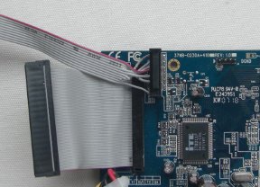
For the PowerPC JTAG connector we have to use a 16-pin plug
(0.1 inch IDC header female connector) where
we only connect the wires which are needed, like on the right
picture. Remove the upper half of the plug so you can press the
wires with your finger or a tool into the blades. Look for a small
arrow on the plug. Position the plug in a way that the arrow is on
the left side, then the leftmost blade indicates pin 1. Pin 2 is
on the upper right of it, then pin 3 on the lower right, etc.
| Altera Pin | JTAG plug Pin |
|---|
| 1 | 7 |
| 2 | 12 |
| 3 | 1 |
| 4 | 6 |
| 5 | 9 |
| 9 | 3 |
| 10 | 16 |
|
Connect the wires from the ribbon cable, as shown in the picture,
using the table. The lines 6, 7 and 8 of the ribbon cable are
not needed and can be cut.
Check both ends of the cable with a multimeter, to make sure
the correct pins are connected. Then finish and close the plug as
usual, for example by exerting pressure on it with a vise.
After that check the cable again. It happens frequently that a
wire has bad contact when building the plug this way.
|
|
|
|
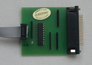
Now the Byteblaster cable (on the left a ByteblasterMV card for the
parallel port from
Individual Computers) can be connected to the target board.
|
|
Compiling UrJTAG
You can get UrJTAG at
http://www.urjtag.org/. The last release will probably be very old,
so you should download a recent version directly from
SVN, using an svn client.
Check out the source like this:
$ svn co https://urjtag.svn.sourceforge.net/svnroot/urjtag urjtag
Note that when downloading a development snapshot from SVN you have to
rebuild the auto configuration files yourself first. You need
autoconf, automake and autopoint. Then run:
$ autoreconf -i -s -v -f
When running under FreeBSD, Linux or Windows you might find a
suitable parallel port driver in UrJTAG, but for NetBSD, at this
writing, there is none. We have to patch the source to add a NetBSD driver
for ppbus. Also make sure that your kernel has ppbus
support and attaches gpio* at ppbus?. Your kernel
config file should include:
ppbus* at atppc?
gpio* at ppbus?
This will make all 17 controllable parallel port pins available as GPIO pins
via /dev/gpio0. Next, patch the UrJTAG source using
this diff file. The diff is based on SVN
r2012 and may not apply cleanly to other revisions. It adds a gpio
lowlevel driver which can control all pins.
Alternatively you can download the already patched and reconfigured
r2012 source archive from
here.
Now you can run the auto configuration and select at least the
mpc824x bus driver, the byteblaster cable driver and
the gpio lowlevel driver (or anything appropriate, when not
running NetBSD):
$ ./configure --disable-nls --enable-bus=mpc824x --enable-cable=byteblaster --enable-lowlevel=gpio --disable-svf
Compile the application with GNU-make (gmake). If nothing goes
wrong you will get a program called jtag. Install everything
with gmake install (default installation path is
/usr/local/).
First run
Start UrJTAG with the jtag command and configure your cable.
You may have to fix the permissions of /dev/gpio0 or start UrJTAG
as root.
Then run the detect command. If UrJTAG could establish a
connection to the CPU it will immediately print the length of the
instruction register (IR) and the chain length (number of
devices which are controllable by JTAG). A message like
"Device Id: not supported" is normal for the MPC824x. We will
have to include the 8241 signal definitions manually with the
include command.
UrJTAG 0.10 #2012
Copyright (C) 2002, 2003 ETC s.r.o.
Copyright (C) 2007, 2008, 2009 Kolja Waschk and the respective authors

UrJTAG is free software, covered by the GNU General Public License, and you are
welcome to change it and/or distribute copies of it under certain conditions.
There is absolutely no warranty for UrJTAG.

warning: UrJTAG may damage your hardware!
Type "quit" to exit, "help" for help.

jtag> cable ByteBlaster gpio /dev/gpio0
Initializing gpio port /dev/gpio0
jtag> detect
IR length: 8
Chain length: 1
Device Id: not supported (bit 0 was not a 1)
jtag>
This is already a big step and half the way to success.
If something goes wrong the detect command will be busy
for a very long time and print nothing, or will result in an error
message like "TDO seems to be stuck".
The latter is worse and means that either your cable is bad or that the
JTAG interface on the target board is not working. In the first case
it sometimes helps to powercycle the target board and rerun the
detect command.
Check and fix UrJTAG's mpc824x bus driver
Up to the latest revision (r2012) there is a bug in UrJTAG's mpc824x bus
driver, which makes it impossible to detect any flash chip on the bus.
The following happens, when running UrJTAG:
UrJTAG 0.10 #2012
Copyright (C) 2002, 2003 ETC s.r.o.
Copyright (C) 2007, 2008, 2009 Kolja Waschk and the respective authors

UrJTAG is free software, covered by the GNU General Public License, and you are
welcome to change it and/or distribute copies of it under certain conditions.
There is absolutely no warranty for UrJTAG.

warning: UrJTAG may damage your hardware!
Type "quit" to exit, "help" for help.

jtag> cable ByteBlaster gpio /dev/gpio0
Initializing gpio port /dev/gpio0
jtag> detect
IR length: 8
Chain length: 1
Device Id: not supported (bit 0 was not a 1)
jtag> include motorola/mpc8241/1.2
   Using default bus width 8
jtag> detectflash 0xffc00000
dev ID=0090   man ID=0090
urj_flash_amd_detect: mid 90, did 90
error: flash: mid != 0x01
According to the
MPC8245UM the flash memory should be connected to the data bus
bit 0-7 (for 8 bit mode) or bit 0-15 (for 16 bit mode). These are the
most significant bits in PowerPC notation. Unfortunately UrJTAG tries to
write to the mpc824x bus using the least significant data lines. When
switching the bus to 32 bits you can see the flash data appear in
the MSB:
jtag> initbus mpc824x width=32
Initialized bus 1, active bus 0
jtag> bus 1
jtag> peek 0xffc00000
URJ_BUS_READ(0xffc00000) = 0xD7FFFFFF (-671088641)
jtag> peek 0xffc00004
URJ_BUS_READ(0xffc00004) = 0xC1FFFFFF (-1040187393)
jtag> peek 0xffc00008
URJ_BUS_READ(0xffc00008) = 0xEFFFFFFF (-268435457)
jtag> peek 0xffc0000c
URJ_BUS_READ(0xffc0000c) = 0x68FFFFFF (1761607679)
The following patch fixes that. It is already
included in the source archive mentioned above:
--- /home/frank/src/urjtag/src/bus/mpc824x.c	2011-11-19 18:05:02.000000000 +0100
+++ mpc824x.c	2011-11-20 20:42:38.000000000 +0100
@@ -402,10 +402,15 @@
     if (area.width > 64)
         return;

+#if 0
     for (i = 0; i < area.width; i++)
         urj_part_set_signal (p, D[i], 1,
                              (d >> ((REVBITS == 1) ? BUS_WIDTH - 1 - i : i)) &
                              1);
+#else
+    for (i = 0; i < area.width; i++)
+        urj_part_set_signal (p, D[24+i], 1, (d >> i) & 1);
+#endif

     /* Just for debugging */
     if (dbgData)
@@ -451,9 +456,17 @@
     if (area.width > 64)
         return 0;

+#if 0
     for (i = 0; i < area.width; i++)
         d |= (uint32_t) (urj_part_get_signal (p, D[i]) <<
                          ((REVBITS == 1) ? BUS_WIDTH - 1 - i : i));
+#else
+    for (i = 0; i < 32; i++)
+        d |= (uint32_t) (urj_part_get_signal (p, D[i]) <<
+                         ((REVBITS == 1) ? BUS_WIDTH - 1 - i : i));
+    /*printf("databus: %08x\n",d);*/
+    d >>= 24; /*XXX*/
+#endif

     /* Just for debugging */
     if (dbgData)
This is just a hack to fix the 8-bit mode. Others will still
fail. Also the REVBITS mode no longer works.
Detect the flash
After setting the cable and loading the mpc8241 JTAG support code we
can detect the flash at 0xffc00000 (as it is a 4MB flash):
UrJTAG 0.10 #2012
Copyright (C) 2002, 2003 ETC s.r.o.
Copyright (C) 2007, 2008, 2009 Kolja Waschk and the respective authors

UrJTAG is free software, covered by the GNU General Public License, and you are
welcome to change it and/or distribute copies of it under certain conditions.
There is absolutely no warranty for UrJTAG.

warning: UrJTAG may damage your hardware!
Type "quit" to exit, "help" for help.

jtag> cable ByteBlaster gpio /dev/gpio0
Initializing gpio port /dev/gpio0
jtag> detect
IR length: 8
Chain length: 1
Device Id: not supported (bit 0 was not a 1)
jtag> include motorola/mpc8241/1.2
   Using default bus width 8
jtag> detectflash 0xffc00000
Query identification string:
        Primary Algorithm Command Set and Control Interface ID Code: 0x0002 (AMD/Fujitsu Standard Command Set)
        Alternate Algorithm Command Set and Control Interface ID Code: 0x0000 (null)
Query system interface information:
        Vcc Logic Supply Minimum Write/Erase or Write voltage: 2700 mV
        Vcc Logic Supply Maximum Write/Erase or Write voltage: 3600 mV
        Vpp [Programming] Supply Minimum Write/Erase voltage: 0 mV
        Vpp [Programming] Supply Maximum Write/Erase voltage: 0 mV
        Typical timeout per single byte/word program: 16 us
        Typical timeout for maximum-size multi-byte program: 0 us
        Typical timeout per individual block erase: 1024 ms
        Typical timeout for full chip erase: 0 ms
        Maximum timeout for byte/word program: 512 us
        Maximum timeout for multi-byte program: 0 us
        Maximum timeout per individual block erase: 16384 ms
        Maximum timeout for chip erase: 0 ms
Device geometry definition:
        Device Size: 4194304 B (4096 KiB, 4 MiB)
        Flash Device Interface Code description: 0x0002 (x8/x16)
        Maximum number of bytes in multi-byte program: 1
        Number of Erase Block Regions within device: 2
        Erase Block Region Information:
                Region 0:
                        Erase Block Size: 8192 B (8 KiB)
                        Number of Erase Blocks: 8
                Region 1:
                        Erase Block Size: 65536 B (64 KiB)
                        Number of Erase Blocks: 63
Primary Vendor-Specific Extended Query:
        Major version number: 3
        Minor version number: 3
        Address Sensitive Unlock: Required
        Process Technology: 170-nm Floating Gate technology
        Erase Suspend: Read/write
        Sector Protect: 1 sectors per group
        Sector Temporary Unprotect: Not supported
        Sector Protect/Unprotect Scheme: 29BDS640 mode (Software Command Locking)
        Simultaneous Operation: 48 sectors
        Burst Mode Type: Supported
        Page Mode Type: Not supported
        ACC (Acceleration) Supply Minimum: 8500 mV
        ACC (Acceleration) Supply Maximum: 12500 mV
        Top/Bottom Sector Flag: Bottom boot device
        Program Suspend: Supported
        Unlock Bypass: Supported
        SecSi Sector (Customer OTP Area) Size: 0 bytes
        Embedded Hardware Reset Timeout Maximum: 0 ns
        Non-Embedded Hardware Reset Timeout Maximum: 0 ns
        Erase Suspend Timeout Maximum: 0 us
        Program Suspend Timeout Maximum: 0 us
When you can read this on your terminal then you have won. The flash
is responding and can be reprogrammed with a new bootloader.
Write a new bootloader to the flash
Get a suitable PPCBoot or UBoot bootloader for your MPC824x board.
For the Allnet 6250 you find it in the official
GPL archive from Allnet (ppcboot/ppcboot.bin).
jtag> flashmem 0xfff00000 ppcboot.bin noverify
You may want to add noverify to save time. Writing a 100K PPCBoot
image to flash can last up to 5 hours over JTAG!
Frank Wille, November 2011